Next | Prev | Up | Top | Contents | Index
VME Hardware Features and Restrictions
When designing an OEM hardware board to interface to the Challenge or Onyx VME bus, observe the following restrictions:
- Devices should require 8-bit interrupt vectors only. This is the only interrupt vector size that is supported by the VMECC or recognized by the IRIX kernel.
- Devices must not require UAT (unaligned transfer or tri-byte) access.
- Devices in slave mode must not require address modifiers other than Supervisory/Nonprivileged data access.
- While in master mode, a device must use only nonprivileged data access or nonprivileged block transfers.
- The Challenge or Onyx VME bus does not support VSBbus boards. In addition, there are no pins on the back of the VME backplane. This area is inaccessible for cables or boards.
- Metal face plates or front panels on VME boards may prevent the I/O door from properly closing and can possibly damage I/O bulkhead. (In some VME enclosures, a face plate supplies required EMI shielding. However, the Challenge chassis already provides sufficient shielding, so these plates are not necessary.)
Designing a VME Bus Master for Challenge and Onyx Systems
The following notes are related to the design of a VME bus master device to work with a machine in the Challenge/Onyx series. A VME bus master, when programmed using the functions described in "Mapping DMA Addresses", can transfer data between itself and system memory.
The setup time at the start of a DMA transfer is as follows:
- First word of a read is delivered to the master in 3 to 8 microseconds.
- First word of a write is retrieved from the master in 1 to 3 microseconds.
The F controller does the mapping from A32 mode into system memory and automatically handles the crossing of page boundaries. The VME Bus Master is not required to make AS go high and then low on 4 KB boundaries. However, when using A64 addressing, the device may have to change the address on the 4 KB boundaries and cause a transition on AS low to high, and then back to low. This incurs new setup delays.
The important parts of the VME handshake cycle are diagrammed in Figure 13-4.
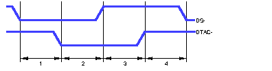
Figure 13-4 : VMECC Contribution to VME Handshake Cycle Time
Intervals 1 and 3 represent the response latency in the bus slave (the VMECC). Intervals 2 and 4 represent the latency in the VME Bus Master. In the Challenge and Onyx systems,
- part 1 is approximately 40 nanoseconds
- part 3 is approximately 25 nanoseconds
The total contribution by the VMECC is approximately 65 nanoseconds. If the total of the four intervals can be held to 125 nanoseconds, the absolute peak transfer rate (in D64 mode) is 64 MB per second.
Note: Startup and latency numbers are averages and may occasionally be longer. The system design does not have any guaranteed latency.
The VME specification provides for a burst length of 265 bytes in D8, D16, and D32 modes, or 2 KB in D64. The burst length is counted in bytes, not transfer cycles.
Operating at this burst length, the duration of a single burst of 2 KB would be 256 transfers at 125 nanoseconds each, plus a startup of roughly 5 microseconds, giving a total of 37 microseconds per burst. Continuous, back-to-back bursts could achieve at most 55 MB per second.
However, the Challenge and Onyx VMECC uses a 20-bit burst counter allowing up to 2 MB in a burst of any data size. Suppose the bus master transfers 64 KB per burst, transferring 4-byte data words. The duration of a single burst would be 8,192 times 125 nanoseconds, plus 5 microseconds startup, or 1,029 microseconds per burst. Continuous bursts of this size achieve a data rate of 63.7 MB per second.
The use of long bursts violates the VME standard, and a bus master that depends on long bursts is likely not to work in other computers. If you decide to exceed the VME bus specifications, you should condition this feature with a field in a control register on the VME board, so that it can be disabled for use on other VME systems.
Next | Prev | Up | Top | Contents | Index